Home > Press > Hitachi’s holography electron microscope attains unprecedented resolution:Image acquisition and defocusing correction techniques enable observations of atomic-scale magnetic fields at never-before-seen resolution
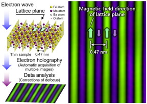 |
| Thanks to advanced image acquisition and automated aberration correction techniques, researchers managed to measure magnetic fields in Ba2FeMoO6 at a groundbreaking resolution of 0.47 nm for a method that enables observation of uneven samples. Such a high resolution is critical when observing magnetic phenomena that occur at the interface between materials. CREDIT Toshiaki Tanigaki from Hitachi, Ltd. |
Abstract:
A research team from Japan, including scientists from Hitachi, Ltd. (TSE 6501, Hitachi), Kyushu University, RIKEN, and HREM Research Inc. (HREM), has achieved a major breakthrough in the observation of magnetic fields at unimaginably small scales. In collaboration with National Institute of Advanced Industrial Science and Technology (AIST) and the National Institute for Materials Science (NIMS), the team used Hitachi’s atomic-resolution holography electron microscope—with a newly developed image acquisition technology and defocus correction algorithms—to visualize the magnetic fields of individual atomic layers within a crystalline solid.
Hitachi’s holography electron microscope attains unprecedented resolution:Image acquisition and defocusing correction techniques enable observations of atomic-scale magnetic fields at never-before-seen resolution
Tokyo, Japan | Posted on July 5th, 2024Many advances in electronic devices, catalysis, transportation, and energy generation have been made possible by the development and adoption of high-performance materials with tailored characteristics. Atom arrangement and electron behavior are among the most critical factors that dictate a crystalline material’s properties. Notably, the orientation and strength of magnetic fields right at the interface between different materials or atomic layers are particularly important, and often help explain many peculiar physical phenomena. Prior to this breakthrough, the maximum resolution at which the magnetic field of atomic layers could be observed was limited to around 0.67 nm, a record set by Hitachi using their cutting-edge holography electron microscope in 2017.
Now, thanks to a large collaborative project, researchers have managed to push this limit even further by addressing a few key limitations in Hitachi’s holography electron microscope. Their findings have been published in the journal Nature on July 03, 2024.
The researchers first developed a system to automate the control and tuning of the device during data acquisition, significantly speeding up the imaging process to a speed of 10,000 images over 8.5 hours. Then, by performing specific averaging operations with these images, they minimized noise to obtain much clearer images containing distinct electric field and magnetic field data.
The challenge addressed next was the correction for minute defocusing, which caused aberrations in the acquired images. “The idea of post-image-capture correction of aberrations we employed is exactly the same as that which had motivated Dr. Dennis Gabor to invent electron holography in 1948. In other words, the methodology was already theoretically established. Until now, however, there had been no technological implementations for such automated correction in off-axis electron holography,” explains Chief Researcher Toshiaki Tanigaki from Hitachi, Ltd. The technique implemented was able to correct for defocusing due to minor focus shifts by analyzing reconstructed electron waves. Thanks to this approach, the resulting images were free of residual aberrations, making the positions and phases of atoms easily discernible with magnetic field.
Leveraging these two innovations, the team performed electron holography measurements on samples of Ba2FeMoO6, a layered crystalline material in which adjacent atomic layers have distinct magnetic fields. Upon comparing their experimental results with simulations, they confirmed that they surpassed the previously set record, managing to observe the magnetic fields of Ba2FeMoO6 at an unprecedented resolution of 0.47 nm. “This result opens doors to direct observations of the magnetic lattices in specific areas, such as interfaces and grain boundaries, in many materials and devices,” comments an excited Tanigaki. “Our study marks the first step towards investigating many veiled phenomena whose existence can be revealed by electron spin configurations in magnetic materials.”
The team expects their remarkable achievement to help solve many scientific and technological challenges. “Our atomic-resolution holography electron microscope will be used by various parties, contributing to advances in a wide range of fields ranging from fundamental physics to next-generation devices. Ultimately, this would pave the way for the realization of a carbon-neutral society through the development of high-performance magnets and highly functional materials that are essential for decarbonization and energy saving efforts,” concludes an insightful Tanigaki, with eyes on the future.
Only time will tell what exciting discoveries and technological leaps await us in light of the insights gathered via improved electron holography microscopy, so keep an eye out!
####
About Hitachi R&D
Hitachi drives Social Innovation Business, creating a sustainable society through the use of data and technology. We solve customers' and society's challenges with Lumada solutions leveraging IT, OT (Operational Technology) and products. Hitachi operates under the 3 business sectors of “Digital Systems & Services” - supporting our customers’ digital transformation; “Green Energy & Mobility” - contributing to a decarbonized society through energy and railway systems, and “Connective Industries” - connecting products through digital technology to provide solutions in various industries. Driven by Digital, Green, and Innovation, we aim for growth through co-creation with our customers. The company’s revenues as 3 sectors for fiscal year 2023 (ended March 31, 2024) totaled 8,564.3 billion yen, with 573 consolidated subsidiaries and approximately 270,000 employees worldwide.
For more information on Hitachi, please visit the company's website at https://www.hitachi.com.
About Chief Researcher Toshiaki Tanigaki from Hitachi, Ltd.
Toshiaki Tanigaki obtained a PhD from Ritsumeikan University in 2004. He joined the Research and Development Group at Hitachi, Ltd. in 2014, where he currently serves as Chief Researcher. He specializes in electron holography and electron microscopy techniques, as well as manufacturing technologies, measurement engineering, nanostructure physics, and nanotechnologically relevant materials. He has been a member of The Japan Society of Applied Physics and The Japan Society of Microscopy for nearly 20 years and has published over 50 major research papers.
Funding information
The development of the atomic-resolution electron microscope was supported by a grant from the Japan Society for the Promotion of Science (JSPS) through the “Funding Program for World-Leading Innovative R&D on Science and Technology (FIRST Program)” initiated by the Council for Science, Technology, and Innovation (CSTI). Further, a part of this research was also supported by the “Core Research for Evolutional Science and Technology (CREST)” program (JPMJCR1664) of JST.
For more information, please click here
Contacts:
Media Contact
Tsuyoshi Arigane
Hitachi R&D
Expert Contact
Toshiaki Tanigaki
Hitachi, Ltd.
Copyright © Hitachi R&D
If you have a comment, please Contact us.Issuers of news releases, not 7th Wave, Inc. or Nanotechnology Now, are solely responsible for the accuracy of the content.
Bookmark:


| Related Links |
| Related News Press |
News and information
![]() FSU researchers develop new methods to generate and improve magnetism of 2D materials December 13th, 2024
FSU researchers develop new methods to generate and improve magnetism of 2D materials December 13th, 2024
![]() Innovative biomimetic superhydrophobic coating combines repair and buffering properties for superior anti-erosion December 13th, 2024
Innovative biomimetic superhydrophobic coating combines repair and buffering properties for superior anti-erosion December 13th, 2024
![]() Groundbreaking research unveils unified theory for optical singularities in photonic microstructures December 13th, 2024
Groundbreaking research unveils unified theory for optical singularities in photonic microstructures December 13th, 2024
Imaging
![]() Turning up the signal November 8th, 2024
Turning up the signal November 8th, 2024
![]() New discovery aims to improve the design of microelectronic devices September 13th, 2024
New discovery aims to improve the design of microelectronic devices September 13th, 2024
![]() Quantum researchers cause controlled ‘wobble’ in the nucleus of a single atom September 13th, 2024
Quantum researchers cause controlled ‘wobble’ in the nucleus of a single atom September 13th, 2024
Possible Futures
![]() Breakthrough brings body-heat powered wearable devices closer to reality December 13th, 2024
Breakthrough brings body-heat powered wearable devices closer to reality December 13th, 2024
![]() FSU researchers develop new methods to generate and improve magnetism of 2D materials December 13th, 2024
FSU researchers develop new methods to generate and improve magnetism of 2D materials December 13th, 2024
![]() Innovative biomimetic superhydrophobic coating combines repair and buffering properties for superior anti-erosion December 13th, 2024
Innovative biomimetic superhydrophobic coating combines repair and buffering properties for superior anti-erosion December 13th, 2024
![]() Groundbreaking research unveils unified theory for optical singularities in photonic microstructures December 13th, 2024
Groundbreaking research unveils unified theory for optical singularities in photonic microstructures December 13th, 2024
Discoveries
![]() How cells repair DNA’s protective barrier: a pathway to address a rare genetic disorder characterized by rapid aging in children December 13th, 2024
How cells repair DNA’s protective barrier: a pathway to address a rare genetic disorder characterized by rapid aging in children December 13th, 2024
![]() Bringing the power of tabletop precision lasers for quantum science to the chip scale December 13th, 2024
Bringing the power of tabletop precision lasers for quantum science to the chip scale December 13th, 2024
![]() Researchers succeed in controlling quantum states in a new energy range December 13th, 2024
Researchers succeed in controlling quantum states in a new energy range December 13th, 2024
![]() Breakthrough brings body-heat powered wearable devices closer to reality December 13th, 2024
Breakthrough brings body-heat powered wearable devices closer to reality December 13th, 2024
Announcements
![]() FSU researchers develop new methods to generate and improve magnetism of 2D materials December 13th, 2024
FSU researchers develop new methods to generate and improve magnetism of 2D materials December 13th, 2024
![]() Innovative biomimetic superhydrophobic coating combines repair and buffering properties for superior anti-erosion December 13th, 2024
Innovative biomimetic superhydrophobic coating combines repair and buffering properties for superior anti-erosion December 13th, 2024
![]() Groundbreaking research unveils unified theory for optical singularities in photonic microstructures December 13th, 2024
Groundbreaking research unveils unified theory for optical singularities in photonic microstructures December 13th, 2024
Interviews/Book Reviews/Essays/Reports/Podcasts/Journals/White papers/Posters
![]() Breakthrough brings body-heat powered wearable devices closer to reality December 13th, 2024
Breakthrough brings body-heat powered wearable devices closer to reality December 13th, 2024
![]() FSU researchers develop new methods to generate and improve magnetism of 2D materials December 13th, 2024
FSU researchers develop new methods to generate and improve magnetism of 2D materials December 13th, 2024
![]() Innovative biomimetic superhydrophobic coating combines repair and buffering properties for superior anti-erosion December 13th, 2024
Innovative biomimetic superhydrophobic coating combines repair and buffering properties for superior anti-erosion December 13th, 2024
Tools
![]() Turning up the signal November 8th, 2024
Turning up the signal November 8th, 2024
![]() Quantum researchers cause controlled ‘wobble’ in the nucleus of a single atom September 13th, 2024
Quantum researchers cause controlled ‘wobble’ in the nucleus of a single atom September 13th, 2024
![]() Faster than one pixel at a time – new imaging method for neutral atomic beam microscopes developed by Swansea researchers August 16th, 2024
Faster than one pixel at a time – new imaging method for neutral atomic beam microscopes developed by Swansea researchers August 16th, 2024
|
|
||
|
|
||
| The latest news from around the world, FREE | ||
|
|
||
|
|
||
| Premium Products | ||
|
|
||
|
Only the news you want to read!
Learn More |
||
|
|
||
|
Full-service, expert consulting
Learn More |
||
|
|
||