Home > Press > Atomic force microscopy in 3D
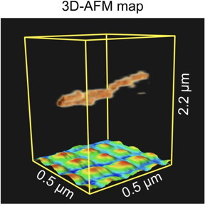 |
| Three-dimensional atomic force microscopy (3D-AFM) map underlining its capability to image suspended flexible samples above a regular pattern of nano-sized dots. CREDIT © 2024 Mohammad Shahidul Alam, et al., Small Methods published by Wiley-VCH GmbH |
Abstract:
Researchers at Nano Life Science Institute (WPI-NanoLSI), Kanazawa University report in Small Methods the 3D imaging of a suspended nanostructure. The technique used is an extension of atomic force microscopy and is a promising approach for visualizing various 3D biological systems.
Atomic force microscopy in 3D
Kanazawa, Japan | Posted on July 5th, 2024Atomic force microscopy (AFM) was originally invented for visualizing surfaces with nanoscale resolution. Its basic working principle is to move an ultrathin tip over a sample’s surface. During this xy-scanning motion, the tip’s position in the direction perpendicular to the xy-plane follows the sample’s height profile, resulting in a height map of the surface. In recent years, ways to extend the method to three-dimensional (3D) imaging have been explored, with researchers from Nano Life Science Institute (WPI-NanoLSI), Kanazawa University reporting pioneering experiments on living cells. However, for 3D-AFM to evolve into a widely applicable technique for visualizing flexible molecular structures, a thorough understanding of the imaging mechanisms at play is necessary. Now, Takeshi Fukuma from Kanazawa University and colleagues have performed a detailed study of a specially designed flexible sample, providing essential insights into the theoretical basis and the interpretation of 3D-AFM experiments.
Using microfabrication tools, the scientists created a sample consisting of a carbon nanotube fiber resting on platinum pillars that in turn were positioned on a silicon substrate. A carbon nanotube is a structure that one can think of as a rolled-up, one-atom-thick carbon sheet. The freestanding portion of the nanotube was about 2 micrometers long. The whole structure was immersed in water, as many 3D biomolecular systems of interest occur in liquid environments.
Fukuma and colleagues then performed 3D-AFM experiments in two different modes. In static mode, the nanotip is lowered vertically towards the sample. When the tip makes contact with the suspended nanotube fiber, the latter gets pushed aside, and bends while the probe descends further. In dynamic mode, the tip, which is attached to a cantilever, is made to oscillate at a resonance frequency while being lowered. By analyzing how the force experienced by the tip changes as a function of the tip’s depth, the researchers concluded that the friction between the tip and the fiber is much larger in static mode compared to dynamic mode. The latter is therefore the mode of choice, as less friction means that potential damage to the sample is less likely.
The scientists performed computer simulations to model what happens when the tip reaches the carbon nanotube fiber. The simulations confirmed that the suspended nanotube displaces laterally, and that a continuously vibrating tip (as in dynamical mode) results in weaker forces experienced by the sample, hindering strong adhesion of the tip to the fiber.
Fukuma and colleagues then performed experiments with a carbon nanotube fiber suspended above a regular pattern of nano-sized platinum dots deposited on a silicon substrate. The measurements were done in dynamical mode. The reconstructed 3D map of the scanned volume clearly showed the fiber and the dots below it, underlining the capability of 3D-AFM to image vertically overlapping nanostructures.
These findings show that AFM can generally be applied to visualize flexible 3D structures. Quoting the scientists: “… the advancements made in this study may potentially lead to more detailed and accurate AFM analysis of various 3D biological systems such as cells, organelles, chromosomes, and vesicles.”
Background
Atomic force microscopy
The principle behind atomic force microscopy (AFM) is to scan the surface of a sample with a very small tip. During this horizontal (xy) scan, the tip, attached to a small cantilever, follows the sample’s vertical (z) profile, which induces a force on the cantilever that can be measured. The magnitude of the force at the xy position can be related to the z value. The xyz data generated during a scan then result in a height map providing structural information about the investigated sample. The cantilever can be made to oscillate near its resonance frequency, which is referred to as dynamic mode AFM. Not letting the cantilever oscillate is known as static mode AFM. In dynamic mode, when the tip is moved around a surface, the variations in the amplitude (or the frequency) of the cantilever’s oscillation — resulting from the tip’s interaction with the sample’s surface — are recorded, as these provide a measure for the local z value.
Takeshi Fukuma and colleagues have now provided a detailed AFM analysis of a 3D reference sample with nanosized features that could be reconstructed with high precision. The experiments and accompanying simulations confirm that AFM has the potential to become a robust method for the characterization of 3D nanosized objects, including biological systems.
Funder
This work was supported by the World Premier International Research Center Initiative, Ministry of Education, Culture, Sports, Science and Technology, Japan; KAKENHI No. 21H05251 and 20H00345, Japan Society for the Promotion of Science and Precursory Research for Embryonic Science and Technology JPMJPR20K6, Japan Science and Technology Agency. The simulations were carried out on the supercomputers at the Research Center for Computational Science in Okazaki, Japan (Project: 23-IMS-C101).
####
About Nano Life Science Institute (WPI-NanoLSI), Kanazawa University
Understanding nanoscale mechanisms of life phenomena by exploring “uncharted nano-realms”
Cells are the basic units of almost all life forms. We are developing nanoprobe technologies that allow direct imaging, analysis, and manipulation of the behavior and dynamics of important macromolecules in living organisms, such as proteins and nucleic acids, at the surface and interior of cells. We aim at acquiring a fundamental understanding of the various life phenomena at the nanoscale.
https://nanolsi.kanazawa-u.ac.jp/en/
About the World Premier International Research Center Initiative (WPI)
The WPI program was launched in 2007 by Japan's Ministry of Education, Culture, Sports, Science and Technology (MEXT) to foster globally visible research centers boasting the highest standards and outstanding research environments. Numbering more than a dozen and operating at institutions throughout the country, these centers are given a high degree of autonomy, allowing them to engage in innovative modes of management and research. The program is administered by the Japan Society for the Promotion of Science (JSPS).
See the latest research news from the centers at the WPI News Portal: https://www.eurekalert.org/newsportal/WPI
Main WPI program site:
www.jsps.go.jp/english/e-toplevel
About Kanazawa University
As the leading comprehensive university on the Sea of Japan coast, Kanazawa University has contributed greatly to higher education and academic research in Japan since it was founded in 1949. The University has three colleges and 17 schools offering courses in subjects that include medicine, computer engineering, and humanities.
The University is located on the coast of the Sea of Japan in Kanazawa – a city rich in history and culture. The city of Kanazawa has a highly respected intellectual profile since the time of the fiefdom (1598-1867). Kanazawa University is divided into two main campuses: Kakuma and Takaramachi for its approximately 10,200 students including 600 from overseas.
http://www.kanazawa-u.ac.jp/e/
For more information, please click here
Contacts:
Hiroe Yoneda
Kanazawa University
nanolsi-office@adm.kanazawa-u.ac.jp
Office: +81-76-234-4550
Copyright © Nano Life Science Institute (WPI-NanoLSI), Kanazawa University
If you have a comment, please Contact us.Issuers of news releases, not 7th Wave, Inc. or Nanotechnology Now, are solely responsible for the accuracy of the content.
Bookmark:


| Related Links |
| Related News Press |
News and information
![]() Closing the gaps — MXene-coating filters can enhance performance and reusability February 28th, 2025
Closing the gaps — MXene-coating filters can enhance performance and reusability February 28th, 2025
![]() Rice researchers harness gravity to create low-cost device for rapid cell analysis February 28th, 2025
Rice researchers harness gravity to create low-cost device for rapid cell analysis February 28th, 2025
Imaging
![]() Turning up the signal November 8th, 2024
Turning up the signal November 8th, 2024
![]() New discovery aims to improve the design of microelectronic devices September 13th, 2024
New discovery aims to improve the design of microelectronic devices September 13th, 2024
![]() Quantum researchers cause controlled ‘wobble’ in the nucleus of a single atom September 13th, 2024
Quantum researchers cause controlled ‘wobble’ in the nucleus of a single atom September 13th, 2024
Govt.-Legislation/Regulation/Funding/Policy
![]() Rice researchers harness gravity to create low-cost device for rapid cell analysis February 28th, 2025
Rice researchers harness gravity to create low-cost device for rapid cell analysis February 28th, 2025
![]() Quantum engineers ‘squeeze’ laser frequency combs to make more sensitive gas sensors January 17th, 2025
Quantum engineers ‘squeeze’ laser frequency combs to make more sensitive gas sensors January 17th, 2025
![]() Chainmail-like material could be the future of armor: First 2D mechanically interlocked polymer exhibits exceptional flexibility and strength January 17th, 2025
Chainmail-like material could be the future of armor: First 2D mechanically interlocked polymer exhibits exceptional flexibility and strength January 17th, 2025
Possible Futures
![]() Closing the gaps — MXene-coating filters can enhance performance and reusability February 28th, 2025
Closing the gaps — MXene-coating filters can enhance performance and reusability February 28th, 2025
![]() Rice researchers harness gravity to create low-cost device for rapid cell analysis February 28th, 2025
Rice researchers harness gravity to create low-cost device for rapid cell analysis February 28th, 2025
Discoveries
![]() Closing the gaps — MXene-coating filters can enhance performance and reusability February 28th, 2025
Closing the gaps — MXene-coating filters can enhance performance and reusability February 28th, 2025
![]() Rice researchers harness gravity to create low-cost device for rapid cell analysis February 28th, 2025
Rice researchers harness gravity to create low-cost device for rapid cell analysis February 28th, 2025
Announcements
![]() Closing the gaps — MXene-coating filters can enhance performance and reusability February 28th, 2025
Closing the gaps — MXene-coating filters can enhance performance and reusability February 28th, 2025
![]() Rice researchers harness gravity to create low-cost device for rapid cell analysis February 28th, 2025
Rice researchers harness gravity to create low-cost device for rapid cell analysis February 28th, 2025
Interviews/Book Reviews/Essays/Reports/Podcasts/Journals/White papers/Posters
![]() Leading the charge to better batteries February 28th, 2025
Leading the charge to better batteries February 28th, 2025
![]() Quantum interference in molecule-surface collisions February 28th, 2025
Quantum interference in molecule-surface collisions February 28th, 2025
![]() New ocelot chip makes strides in quantum computing: Based on "cat qubits," the technology provides a new way to reduce quantum errors February 28th, 2025
New ocelot chip makes strides in quantum computing: Based on "cat qubits," the technology provides a new way to reduce quantum errors February 28th, 2025
Tools
![]() Rice researchers harness gravity to create low-cost device for rapid cell analysis February 28th, 2025
Rice researchers harness gravity to create low-cost device for rapid cell analysis February 28th, 2025
![]() New 2D multifractal tools delve into Pollock's expressionism January 17th, 2025
New 2D multifractal tools delve into Pollock's expressionism January 17th, 2025
![]() Turning up the signal November 8th, 2024
Turning up the signal November 8th, 2024
Grants/Sponsored Research/Awards/Scholarships/Gifts/Contests/Honors/Records
![]() New discovery aims to improve the design of microelectronic devices September 13th, 2024
New discovery aims to improve the design of microelectronic devices September 13th, 2024
![]() Physicists unlock the secret of elusive quantum negative entanglement entropy using simple classical hardware August 16th, 2024
Physicists unlock the secret of elusive quantum negative entanglement entropy using simple classical hardware August 16th, 2024
![]() Aston University researcher receives £1 million grant to revolutionize miniature optical devices May 17th, 2024
Aston University researcher receives £1 million grant to revolutionize miniature optical devices May 17th, 2024
|
|
||
|
|
||
| The latest news from around the world, FREE | ||
|
|
||
|
|
||
| Premium Products | ||
|
|
||
|
Only the news you want to read!
Learn More |
||
|
|
||
|
Full-service, expert consulting
Learn More |
||
|
|
||